The code for this lesson is available on github under the tag ‘lesson_4’. To get the latest code with git, the following commands can be run from the project root directory. Checkout master first since this is the branch that is tracking the origin and contains all the changes.
git checkout master
git pull
git checkout -b lesson_4_devel lesson_4
Part 1: Configuring the clock module
Start the Launchpad programmed with the code from lesson 3. How fast is the LED blinking? What if you wanted to make the LED blink twice a second, what delay would be required? That depends on the frequency of the CPU which is controlled by a clock source, or oscillator, in conjunction with the configurable clock module of the MSP430. There are many types oscillators which range in price and accuracy depending on the application. In general, a higher frequency bus will require a more accurate clock, but there are other factors which can affect accuracy such as temperature and electrical noise which must be taken into account by the hardware designer. Clock sources can be internal or external. External oscillators are usually more accurate, but they add to cost and space on the board. For the purposes of these tutorials, using the internal oscillator shall be sufficient. The MSP430 clock module can have up to four clock sources:
- DCOCLK: Internal digitally controller oscillator
- VLOCLK: Internal very low frequency oscillator (~12kHz)
- LFXT1CLK: Low or high frequency oscillator can be used with an external low frequency crystal (i.e. 32768Hz for a clock) or at high frequency requiring an external crystal, resonator or clock source in the range of 400kHz – 16MHz
- XT2CLK: High frequency oscillator which requires an external crystal, resonator or clock source in the range of 400kHz – 16MHz
Not all devices support all clock sources. The MSP430G2553 does not have an XT2CLK nor does it support the high frequency oscillator mode on LFXT1CLK. These clock sources can be configured to drive the three internal clock signals:
- MCLK: The master clock used by the CPU
- SMCLK: The sub-main clock, used for peripherals
- ACLK: The auxiliary clock, also used for peripherals
On power up or after a reset, the device is configured such that MCLK is sourced from DCOCLK which has a frequency of approximately 1.1MHz. SMCLK is also sourced from DCOCLK and ACLK is sourced from LFXT1CLK. The use of SMCLK and ACLK for peripherals is controlled by software configuration of the specific module. All the clocks have divider options, so even if the source is 16MHz, the clock signal may be half, a quarter or an eighth of the frequency. This is useful if there is only one clock source, say DCOCLK, configured to 16MHz, but the peripherals using SMCLK should only be running at 4MHz.
There are four registers to configure the MSP430 clock module:
- DCOCTL: DCO control
- BCSCTL1: Basic clock system control 1
- BCSCTL2: Basic clock system control 2
- BCSCTL3: Basic clock system control 3
The register fields are illustrated in the diagram below.
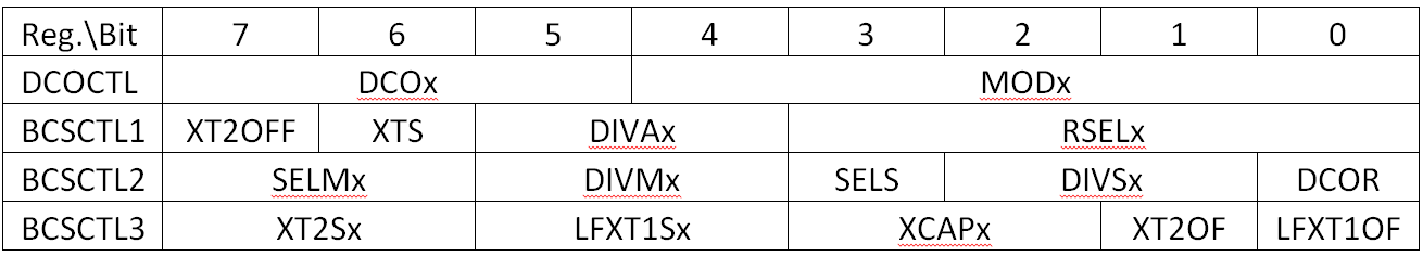
Detailed definitions of these registers can be found in section 5.3 of the family reference manual. The source of the master clock is selected using BCSCTL2[SELMx]. In case you are not familiar with the latter notation, it is read as register[field in the register]. The default value after reset is 0b00, which configures the source to be DCOCLK, therefore no modification is required. Since the DCOCLK will be used as the source, the frequency must be configured. Three fields are required to do so, DCOCTL[DCOx], DCOCTL[MODx] and BCSCTL1[RSELx]. Selecting the values for DCOCTL[DCOx] and BCSCTL1[RSELx] can be done using figure 5-6 in the family reference manual. Choosing MODx is more involved and beyond the scope of this course as it requires knowledge of clock spreading and its effects on electromagnetic interference (EMI).
So what if an MCLK frquency of 1MHz clock is required? Using the values from the figure in the reference manual is not very accurate, and there is no easy way to determine what MODx should be. Luckily TI provides the data for us stored right on the chip. In the last lesson when we looked at the device specific memory organization (table 8 in the datasheet), there was a section in the flash called ‘Information Memory’. This section of the flash contains calibration data that TI has measured and provides to the user for accurate configuration of the device. The data there is stored in what TI calls TLV (Tag-Length-Value) format, which is a table of data at specific offsets defined by tags in the datasheet and reference manual. The TLV data is protected from modification using a software protection mechanism, but the integrity of the data should still be verified before using it. The first 2 bytes of the TLV area (address 0x10c0) contain the checksum of the next 62 bytes which contains the data. The checksum is verified by XOR’ing the data as 16-bit words and then adding the checksum. If the result is zero, the data is valid, any other value means the data is corrupted. Please note, there are many methods of calculating checksums, so this algorithm may not always be applicable. Below is a function which demonstrates how to verify the integrity of information section.
static int _verify_cal_data(void)
{
    size_t len = 62 / 2;
    uint16_t *data = (uint16_t *) 0x10c2;
    uint16_t crc = 0;

    while (len-- > 0) {
        crc ^= *(data++);
    }

    return (TLV_CHECKSUM + crc);
}
There are a few stylistic and code safety notes that are worth mentioning. First of all, the function is declared static and therefore the function name is preceded with an underscore. This is a personal preference and you don’t have to follow it, but it makes it easy to know which functions are only accessible within the file. Next is the use of types size_t and uint16_t. To access these types you must include “stddef.h” and “stdint.h” respectively. I almost always use size_t as an index in loops since it is the type returned by the sizeof operator (sizeof() an array for example). The use of uint16_t is more important however. When the specific length of data is known, it is always safest and considered best practice to use the POSIX types (or equivalent) which clearly indicate the size of the variable. In this case, using ‘unsigned int’ would be the equivalent, but what if the same code was compiled on a PC. That variable would now be 32 bit (or 64 bit) and the code would be incorrect. Of course this code is specific for the MSP430, but the idea applies to any algorithm or calculation. Finally the return type follows the *nix standard where a signed integer is returned such that 0 indicates success and any other value is a failure. Again this is a personal preference but consistency is always good. Using too many return types can be confusing and unless there is a need to know the reason for failure, a simple success or failure status is often adequate.
Now that the calibration data can be validated, let’s take a look at how it can be used to configure the device. The calibration data includes values for 1MHz, 8MHz, 12MHz, and 16MHz based on a 25 degree Celsius ambient temperature. The tags for each frequency setting are stored as two bytes, one contains the value for register DCOCTL and the other for BCSCTL1. Only the fields mentioned above required to configure DCOCLK are set. All other fields in the registers are cleared (except for BCSCTL1[X2OFF] if applicable to the device). To access this calibration data and set the DCOCLK to 1MHz, the following code can be used.
/* Configure the clock module - MCLK = 1MHz */
DCOCTL = 0;
BCSCTL1 = CALBC1_1MHZ;
DCOCTL = CALDCO_1MHZ;
The first line of code clears DCOCTL to set the DCOCLK to the lowest setting. Next the calibration data is copied into the DCOCTL and BCSCTL1 registers respectively using the tags from the TLV area. The DCOCLK is now running at 1MHz. The DCOCLK can also be configured to any of the other supported frequency values in the calibration data using the available tags. Since BCSCTL2 still has its default values the current configuration can be summarized as follows:
- MCLK source is DCOCLK
- MCLK divider is 1, therefore MCLK = DCOCLK = 1MHz
- SMCLK source is DCOCLK
- SMCLK divider is 1, therefore SMCLK = DCOCLK = 1MHz
The only clock is that is not configured is ACLK which can be sourced from either VCOCLK or LFXT1CLK. Currently the frequency of ACLK will be 0Hz, and if it is to be enabled, either it must be sourced from VCOCLK by setting BCSCTL3[LFXT1Sx] = 2, or by installing the external crystal required for LFXT1CLK. I would have recommended using VCOCLK, but after looking in the datasheet, VCOCLK can be anywhere from 4kHz – 20kHz, a range so wide it won’t be practical for any of these tutorials. For now it can be left as is, and if needed in the future, a crystal can be installed and the device configured accordingly.
Part 2: Setting the LED blinking frequency
Now that the CPU frequency is known, the frequency of the blinking LED can be accurately configured. To blink the LED at a specific frequency, the number of CPU cycles to wait between toggling the LED must be calculated. Since the frequency of the CPU is 1MHz, 1 million cycles are executed per second. If the desired blinking frequency is 2Hz (2 toggles per second), the LED should be toggled every 500000 cycles. [Update] As Jerry pointed out in the comments below, my original definition of the frequency was incorrect. A frequency of 1Hz means that the LED should toggle on and off once, since this is the periodic signal. Therefore to correct the sentence above, a frequency of 2Hz would require the LED to be toggled 4 times a second, or every 250000 cycles. The rest of the lesson has been updated to reflect this change. The following formula can be used to calculate the delay:
This calculation can be implemented as a hash define in the code so that it will be calculated automatically. Using the formula above along with the __delay_cycle function, the code from the last lesson can be modified to set the blinking frequency to 2Hz.

/* LED blinking frequency */
#define LED_BLINK_FREQ_HZ 2

/* Number of cycles to delay based on 1MHz MCLK */
#define LED_DELAY_CYCLES (1000000 / (2 * LED_BLINK_FREQ_HZ))
...
while (1) {
    /* Wait for LED_DELAY_CYCLES cycles */
    __delay_cycles(LED_DELAY_CYCLES);

    /* Toggle P1.0 output */
    P1OUT ^= 0x01;
}
Note the following two reasons why a hash define is used to calculate the number of cycles:
- The __delay_cycles function only takes a constant argument. If anything other than a constant is passed as an argument to this function, the compiler will throw an error
- Using the hash define means the value is computed only once by the compiler. This makes the code more efficient. It also means the loop is more accurate, because doing division on an MSP430 could take many clock cycles, causing the delay to be longer than intended
Part 3: Pin Configuration
Last lesson we briefly touched on the topic of pin configuration. Pin P1.0 could be configured as a digital input or a digital output using the P1DIR register. This is only part of the story. Most pins can actually be configured to perform several different functions. This is called pin multiplexing. Almost every microcontroller supports pin multiplexing on pins which do not have a dedicated function. Each pin is different and will have the ability to be configured for a defined set of peripherals on the chip. Often, as is the case with the MSP430, the default configuration of a pin is a digital input. To configure a pin to use one of its alternate functions, the PxSEL1 and PxSEL2 registers are used. These registers follow the same bit to pin mapping as described in lesson 3. When the bit for a given pin is cleared in both of these registers, as they are on reset, the pin is configured as a digital I/O (also called a general purpose input/output, or GPIO). Setting the appropriate bit in either or both of these registers will enable the pin’s alternate functions. The list of alternate functions for each pin can be found in device datasheet starting from table 16. It is important to note that even if a peripheral function is selected for a specific pin, the other port configuration registers (such as PxDIR) may still have to be appropriately configured. When we begin to use the peripheral devices, this concept will become clear.
The GPIOs on the MSP430 also have the option to be connected to internal pull-up or pull-down resistors through the PxREN registers. When the PxREN bit for a specific pin is set, the P1OUT register controls which resistor (pull-up or pull-down) the pin will be connected to. A pin connected to pull-up/pull-down resistors can be still be driven to the any level by an external device. For example, I2C uses pull-up resistors so that the idle state of the line is high. The master drives the line low to begin communication. Internal pull-ups and pull-downs are rarely used in practice as the value is fixed by the implementation of the microcontroller. Most digital designers prefer to have control over the specific value and also the ability to change it if required. The PxREN registers apply even if the pin is configured as an input.
Now lets go through an example to help solidify your understanding of pin configuration. The objective is to modify the code such that the LED will start blinking only once switch 2 (SW2) on the launchpad has been pressed. Switch 2 is connected to pin P1.3. From the datasheet, we can see all the possible functions of this pin.
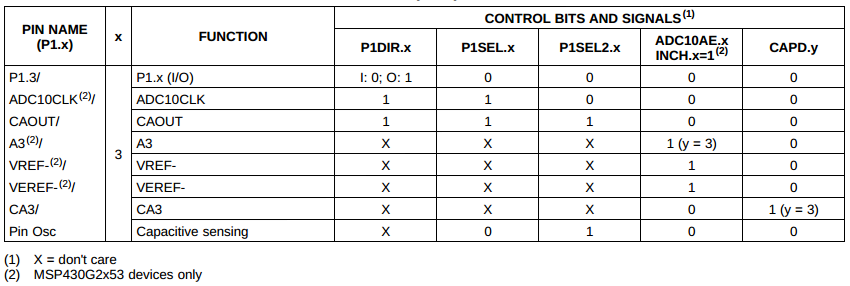 From the MSP430G2553 Datasheet (SLAS735)
Pin P1.3 can be either a GPIO, an ADC clock output, a comparator output or a capacitive sensing input using the P1SEL/2 registers. It can also be configured as an ADC voltage reference or input as well as a comparator input by setting some additional registers, but lets leave these aside for now. The goal is to read a push button, so GPIO functionality is required, therefore P1SEL[3] and P1SEL2[3] should be cleared. Next, P1DIR[3] should be cleared to set the direction as an input. On rev 1.5 Launchpads, TI has removed the external pull-up resistor for the button so we must use the internal one. If your Launchpad is older this will still work. Set P1REN[3] and P1OUT[3] to enable the internal pull-up resistor. Finally, the register P1IN is read to obtain the value of the switch. In the example code below, each of these registers will be explicitly set even if the default value is correct. This is done for code clarity and robustness.
/* Configure P1.3 to digital input */
P1SEL &= ~0x08;
P1SEL2 &= ~0x08;
P1DIR &= ~0x08;

/* Pull-up required for rev 1.5 Launchpad */
P1REN |= 0x08;
P1OUT |= 0x08;

/* Wait forever until the button is pressed */
while (P1IN & 0x08);
Polling a register is a valid way to determine if the input has changed value; however, it is not the best way. While the code sits in an infinite loop waiting for the button to be pressed, nothing else can happen – no other code can be executed. In this simple example, this is not a problem because that is all we want to do. But say you wanted to stop the LED from flashing, when would you read P1IN? If you do it only once per loop, it will only check the value of the pin twice per second. If the button is pushed and released in less than that time, it will not be detected. This is where interrupts come in, and allow the microcontroller to notify the software when the hardware has been changed almost immediately. In the next lesson, we will learn more about the MSP430 architecture which is required to understand how interrupts work. Then in the following lesson we will dive into the very important topic of interrupts.
I’m having some difficulty getting the example program to function correctly. On my board the program should block at:
while (P1IN & 0x08);
but doesn’t. In the debugger the value of register P1IN is always 0. The register value does not change when the switch is pressed.
What value should register P1IN have at startup?
Also, the line “P2SEL &= ~0x08;” is a bit confusing to me. Why is P2SEL (Port 2 Selection) set, when port 1 is being configured?
Hi Joel. Let’s start with your last question first, because there is a simple answer. I made a mistake and accidentally left some extra code I was testing with in the master branch. It doesn’t really change anything by being there since currently we have nothing on that port, but it was incorrect. Thanks for pointing it out. I have fixed the code and pushed a new tag for this lesson. To get the latest checkout the master branch and do a ‘git pull’.
As for the first part of your question with regards to the while loop and P1IN. You are right, the board should spin at the while loop until you press the button. The value of P1IN shouldn’t always be zero. When I run the code and have not pressed the button, the value of P1IN is 0x0F. To read P1IN, you have to CTRL^C the program and then type ‘md 0x0020’. The first byte will be P1IN. To see that value change, break the program, then press the button and hole it while to type ‘md 0x0020’ again. Does the value change?
I finally got the program to work. After the update P1IN was still 0x00 after configuring P1.3. The following statements seem to work though:
P1SEL &= ~0x08;
P1DIR &= ~0x08;
P1REN |= 0x08;
P1OUT |= 0x08;
That’s interesting. What you did makes sense if there is no external pull-up. What revision launchpad do you have? I am using a rev 1.4. I would like to compare the schematics and see if they changed anything.
I have the revision 1.5.
I should clarify on thing though, after re-reading my previous comments I noticed that I wasn’t completely accurate. I meant to state that register P1IN bit 3 (P3) was zero. Bits 0 (P0), 1 (P1) and 2 (P2) were set to one. After adding the new statements the register P1IN was equal to 0x0F when waiting for the button press.
Thanks for the clarification. Other then the difference on P1.3, I had the same values. I looked into the schematics and there should be a pull-up resistor connected to P1.3 on rev 1.5 boards (same as on rev 1.4). Do you have a multimeter? If so, I suggest you try the following to see if your board is damaged. Take the main.c from the tutorials, comment out or delete all the code after holding the watchdog (the first line) and put an empty while(1) loop. Compile and program it to the device. Now run the code and measure P1.3 vs ground. It should be above 3V. If its not, remove power from the board, put the multimeter in Ohms mode and test the resistance across R34 (should be marked on the board, its right above the left header). It should be 47K.
I’ve got rev 1.5 and can confirm the behavior described by Joel (i.e. I need P1.3 resistor enabled and P1OUT.3=1 to enter the first while loop). Why does the output value have to be set when the pin’s set as input ? I also get P1IN=0x06 without the buttons pressed which doesn’t change on button press. But if I add the two lines Joel suggested then the value of P1IN changes from 0x4f to 0x47. I’ve got a multimeter so will check for board damage next. Thanks for the very good lessons.
Ignore the question about why P1OUT.3 needs to be set when P1.3 is configured as input. States above it controls which resistor (up/down) to which the pin connects.
Sorry I don’t have a multimeter. The changes for revision 1.5 are described in the launchpad user’s guide though (section 1.4). Looks like the pullup resistor was removed to save power.
Good find. I was looking at the schematic and its still there but as you said in the user guide they said its removed so it must be. I am surprised they didn’t remove it from the schematic or mark it as NE (not equipped). I made the changes you made on my board and it still works – which is what I expected. I will push the changes to the repository. I will also try to get my hands on a rev 1.5 so I can be testing the code on both.
The pads for the external pull up resistor on P1.3, as well as a cap, are still in place on the circuit board but no surface mount resistor (or cap) is in place.
Yes, I suppose TI figured it made more sense just to NE those two components instead of changing the layout. That way if someone wants they could populate R34 and C24 themselves and disable the internal pull-ups. Good point, thanks for mentioning it!
Since the next lesson is on interrupts, can I please ask for your assistance with solving a problem I’m facing with the out-of-box (oob) temperature example ? I’ve been able to successfully compile the the CCS/Windows oob temperature example and run the GUI to display the data. I made some changes to the interrupt definitions ( __attribute__((interrupt (TIMER_A0_VECTOR))) void Timer_A(void) ) in the msp430-gcc version of the same code to run on Linux. The code compiles and loads and the button interrupt works. On linux, I’m trying to use screen to see the temperature data that the launchpad is sending via serial. The manual lists the baud rate as 2400 but ‘screen -nf /dev/ttyACM0 2400’ gives a stream of question marks when the button is pressed. I’ve tried to look through the screen manual to change other settings (cs7/cs8) but all I ever get are question marks. I think the baud rate is correct (2400) because any other baud rate and I don’t even get question marks. Any suggestions for the screen settings ?
Hi Sridhar,
Sorry for the delay in getting back to you. I have never used the screen utility for reading terminal output, my personal preference is minicom. You can download it from the repository. To configure it you will have to do some setup.
sudo apt-get install minicom
sudo minicom -s
Scroll down to “Serial Port Setup”
Press “A” to change the device
Type in the device name
Press enter
Press “E” to change the baud rate
Press “P” to scroll backwards through the baudrate list until you get to 2400
Press “F” to disable hardware flow control
Press enter
Scroll down to “Save setup as dfl” and press enter
Scroll down to “Exit” and press enter
Now restart minicom with sudo and see if it your application works.
Thanks for the response. I’ll give minicom a go – will update with results.
When I try to do
git checkout master
git pull
git checkout -b lesson_4 lesson_4_devel
the last line results in the error message
fatal: Cannot update paths and switch to branch ‘lesson_4’ at the same time.
Did you intend to checkout ‘lesson_4_devel’ which can not be resolved as commit?
I am not familiar with git and do not know what this means, or what to do to get rid of this error.
OK – it seems that the order of the checkout arguments is incorrect at the top of this page. Instead of
git checkout -b lesson_4 lesson_4_devel
one should write
git checkout -b lesson_4_devel lesson_4
Hi Sakari,
Yes you are absolutely right. That was a error on my part – thanks for brining it to my attention. When creating a new branch, the command should be:
git checkout -b
I believe there is an error in the delay calculation. With a 1 MHz clock rate, a delay of 500k cycles results in a 1 Hz signal since the loop applies a constant value (1 or 0) for that number of cycles, a full period is then twice that cycle count. The delay count should be 1e6/(2*f_desired).
You are right. I was thinking that frequency refers to each toggle (transition) of the LED, while as you point out, the frequency should be referring to the periodic signal which goes on and then off. Therefore the formula you present is correct. I will fix this in the lesson and in the code. Thanks for pointing it out.
“It is a great resource for hobbyists, novice programmers, CS/EE students and hardware designers alike who could benefit from a better understanding of software. ” that’s quite true.
Believe me, this is the greatest resource about MSP430 I’ve ever met ( my favorite reference).
thanks a lot …. you’re a great man.
Thanks younis, appreciate the feedback!