Often there is a need for multiple components on a board to communicate with each other. Say for example, we have some type of sensor and want to obtain the data from the sensor on the microcontroller. The communication between them may not necessarily require high speeds or a long range. One of the most common solutions to solve this problem is I2C, or inter-integrated circuit. I2C is a serial communication bus which uses two wires – one clock and one [bidirectional] data line. It is a master-slave protocol, meaning there must be at least one master and at least one slave on the bus. The master always initiates transactions. The I2C specification was originally created by Phillips and it defines both the physical layer – the electrical signalling – and the protocol. The protocol makes use of the hardware signalling to frame transactions which include an address, read/write (R/W) bit and data. There exist other two wire interfaces which are similar to or even derived from I2C such as SMBus, PMBus, etc… Sometimes they can be compatible, but other times they are not. It is best to ensure that the device you have is specifically I2C compatible.
Of the two signals on an I2C bus, one is the clock (SCL) and the other the data (SDA). The clock is always driven by the master, while the data is bidirectional, meaning it can be driven by either the master or the slave. Both signals are open drain and therefore high impedance (think open circuit) unless driven. A pull-up resistor is required on each line to pull it high in the idle state. When a device drives either of the lines, the open drain output pulls the line low. This design has the advantage that it can support bus arbitration without the chance of bus contention at the electrical level. In other words, if two devices are driving the line, they will not physically damage each other. This is especially useful in multi-master mode – which is defined by the standard – when there are multiple masters communicating with the same or different slaves on the same bus. Bus arbitration (which master has control of the bus) is supported by the physical interface using the open drain design.
The disadvantage however, is that the the bus speed is limited especially over distance and across multiple devices (the limiting factor is in fact capacitance – max 400pF). Therefore, the speed originally specified in the I2C bus standard was 100kHz. Almost all I2C devices will support this rate. However, because higher speeds are obviously desirable, fast mode was introduced to increase the supported rate up to 400kHz. Most devices support these two standard modes. There are higher speed modes as well, but the speed of the bus is determined by the slowest device on the bus, as well as the PCB design and layout.
The voltage levels of I2C are not defined by the specification. Instead it defines a high or low symbol relative to Vcc. This makes the bus flexible in the sense that devices powered with 5V can run I2C at 5V, while devices that run on 3.3V can communicate at 3.3V. The pitfall comes when devices are powered at different levels and need to communicate with each other. You cannot connect a 5V I2C bus to a 3.3V device. For this scenario the design would require a voltage level shifter on the I2C bus between the two devices. Voltage level shifters specifically designed for I2C applications are available.
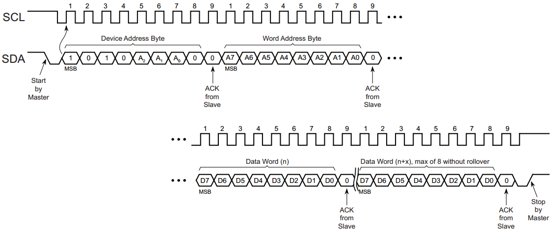
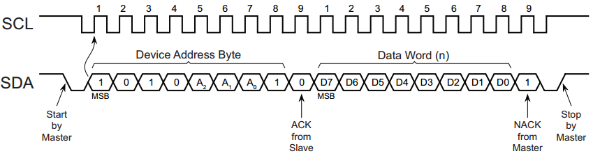
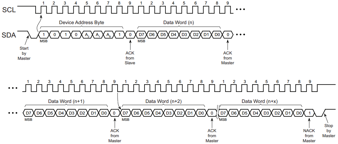
The I2C protocol is defined by a set of conditions which frame a transaction. The start of a transmission always begins with a START condition during which the master leaves SCL idle (high) while pulling SDA low. The falling edge of SDA is the hardware trigger for the START condition. Now all the devices on the bus are listening. Conversely, a transaction is ended with a STOP condition, where the master leaves SCL idle and releases SDA so it goes high as well. In this case, the rising edge of SDA is the hardware trigger for the STOP condition. A STOP condition can be issued at any time by the master.

I2C-bus specification and user manual (UM10204)
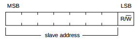
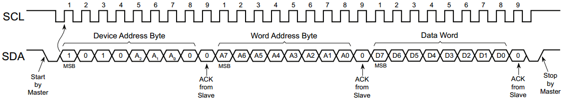
Immediately after the START, the master must send a single byte which comprises of the device address and the read/write (R/W) bit. The device address is the first 7 bits (the most significant bits) while R/W is always bit 0.
I2C-bus specification and user manual (UM10204)
It is important to remember that the address of a device is sometimes provided already shifted left by one while the hardware may expect the unshifted address. Other times the unshifted address may be provided, but the hardware expects the shifted address. This is the most often error when a device does not respond.
The R/W bit indicates to the slave whether the master will be – well – reading or writing to/from the slave device. It determines the direction of transmission of the subsequent bytes. If it is set to read (high) the slave will be transmitting, while if it set to write (low) the master will be transmitting.
The address is transmitted most significant bit first. A single bit is transmitted on SDA for each clock cycle on SCL – therefore transmitting a byte takes 8 clock cycles. After each byte is sent or received, the 9th clock cycle is reserved for the ACK/NACK (acknowledge/not acknowledge) symbol. Depending on the transaction, an ACK can be driven by the either the master or the slave. To signal an ACK, the device pulls SDA low on the 9th clock cycle, while the other device reads the state of the line. If it is low, it is interpreted as an ACK, if it left idle a NACK.
![]()
I2C-bus specification and user manual (UM10204)
For the case when the device address is transmitted, the slave device with the matching address should respond with an ACK. If there is no device on the bus with a matching address, the master will receive a NACK and should end the transaction.
Next comes the data. The data transmitted or received can be as small as one byte up to as many bytes supported by the slave device. Typically a slave should NACK any data byte if it unable to accept any more or if it is busy. The transmitting device must stop transmitting upon receiving the NACK. Once the number of bytes requested has been written or read, the master completes the transaction with the STOP condition.
The standard defines three transaction formats:
- Master transmitter slave receiver – the master sends the first byte with the R/W bit cleared (write). All subsequent data bytes are transmitted by the master and received by the slave.
- Master receiver slave transmitter – the master sends the first byte with the R/W bit set (read). All subsequent data bytes are transmitted by the slave to the master.
- Combined format – effectively format 1 + 2 consecutively with no STOP condition in the middle. Instead of the STOP, there is what is called a repeated START condition which is exactly the same as a START but not preceded by a STOP.
The slave device
Before we move onto implementing the driver, lets take a look at the slave device we will be communicating with. A very commonly used I2C device is the EEPROM. EEPROMs are typically used to store small amounts of data which don’t change very often such as serial number, hardware revision, manufacturing date, etc… The specific EEPROM we will be using is the Atmel AT24C02D, a 2Kb EEPROM with up to 1 million write cycles and can operate at speeds up to 1MHz. Keep in mind that memory devices are often advertised in terms of bits and not bytes, so 2Kb = 2 kilobits, which is (2048/8) 512 bytes – not that that much memory. Even though it has an endurance of 1 million write cycles (meaning the device is guaranteed to be able to perform at least 1 million writes before failing), writing to an EEPROM is quite slow so it is not really intended to be used to store data at runtime.
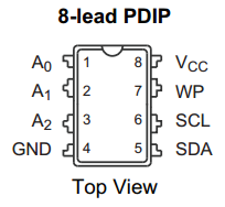
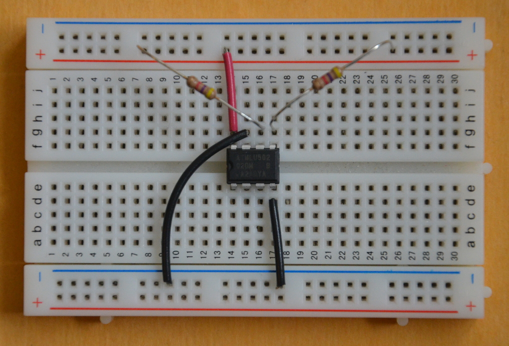
One of the reasons I choose this device is because it is available in a DIP package so it is easy to breadboard. Taking a look at the datasheet, we can see the package description and pin layout for the DIP.
Atmel AT24C02D Datasheet (Atmel-8871E)
Pins 1 – 3 are the customizable address bits A0 – A2 for the I2C device address. The top 4 bits (A3 – A6) are hard coded in the device (we’ll see what these are shortly). Let’s say a hardware designer needs three EEPROMs on the same I2C bus. If they all had the same address, all the devices would respond to every request – obviously not desirable. These pins allow the designer to change the lower three bits of the address so up to eight of these devices can coexist on the same bus. These pins are internally pulled to ground inside the device, so we can leave them not connected unless you want to change the address (although Atmel does recommend connecting them when possible). Pin 4 is the ground pin, so that will be connected that to the ground rail. Pins 5 and 6 are the I2C lines – these will be connected to the MSP430’s SCL and SDA pins which we will configure in software. However, as we learned previously, they require pull-up resistors. Typical values for pull-up resistors on an I2C bus range from 4.7kOhms to 10kOhms. We will use 4.7kOhms for this the breadboard circuit. Pin 7 is the write protect signal. Because EEPROMs are often used to store static data that should never change (i.e. a serial number or a MAC address), the designer can ensure the contents cannot be overwritten by pulling the write protect line high in hardware. Since we want to be able to write to the EEPROM, we will tie this pin to ground. Finally pin 8, Vcc, will be connected to the Vcc rail. With all this connected so far, the breadboard looks like this:
Now let’s take a look at the device address in section 7 of the EEPROM datasheet. Since we left pins A0 – A2 floating, the lower 3 bits of the address will be 0b000. The datasheet specifies that the upper 4 bits will be 0xA (0b1010). This is the diagram provided:

Atmel AT24C02D Datasheet (Atmel-8871E)
So your initial thought might be that we have to address the device as 0xA0. Although this is what the datasheet implies and what is physically transmitted, it is not technically correct. The actual device address should not include the R/W bit. Therefore it should be shifted right by 1 making it 0b1010000 = 0x50. This will be important when we implement the driver.
Most I2C EEPROMs typically support the same types of transactions. The master device can either write to or read from the EEPROM. Writing to the EEPROM can take two forms: byte write and page write. Both require that the first data byte is the address to write to. For example, if the master wants to write to address 0x10, the first data byte will be 0x10. This address is stored in the EEPROMs internal current address register. The next data byte is the actual value to write to the EEPROM. Upon receiving this byte, the EEPROM should respond with an ACK. If the master than sends a STOP, this transaction is a byte write.
Atmel AT24C02D Datasheet (Atmel-8871E)
The master also has the option to continue sending data to the slave, until either the EEPROM responds with a NACK – indicating it is busy – or a full page is written. This is called a page write.
Atmel AT24C02D Datasheet (Atmel-8871E)
A page write need not transmit a full page however. It is up to a page of data that can be written in a single transaction. In the case of the AT24C02D, the page size is 8 bytes. After each byte is received, the current address register in the EEPROM is incremented automatically. However, only the 3 least significant bits in the address will increment. If the master sends more than 8 bytes, those bits will wrap around and the first address will be overwritten. It is therefore important to limit each transaction to a maximum of 8 bytes and then a new transaction with the updated address (incremented by 8 each time) be initiated. Note that both byte write and page writes are of the transaction format 1 – master transmitter slave receiver.
Reading data back from the EEPROM can be performed using one of 3 operations: current address read, random address read and sequential read. The current address read makes use of the EEPROM’s current address register to read the next address in the device. Like writes, each byte that is read increments the current address. However, instead of the address wrapping around a single page, it wraps across the whole device memory space. After one byte is read, if the master issues a NACK it is done reading data and it should subsequently send a STOP.
Atmel AT24C02D Datasheet (Atmel-8871E)
However, if the master responds with an ACK after the first data byte, it will be expecting more data. This current address read becomes a sequential read, which basically means that multiple bytes are read out of the slave device. The master will continue to ACK each data byte until it is done receiving the number of bytes it requires. On the last data byte it must respond with a NACK and then a STOP condition.
Atmel AT24C02D Datasheet (Atmel-8871E)
Notice that both current address read and sequential read (when following a current address read) are in the transaction format 2 – master receiver slave transmitter.
But what if we need to read from a specific address – which is most often the case? This is where message format 3 – combined format – comes into play with the random address read. First the master transmits the device address with the R/W bit set to write and one data byte containing the address to read from. Then it invokes a repeated START condition, changes direction to read and reads a single byte from the EEPROM.

Atmel AT24C02D Datasheet (Atmel-8871E)
Sequential mode can also be applied to the random address read. Just like with the current address read, instead of NACKing the first byte, the master continues to ACK until it has read the desired number of bytes.
I2C with the USCI Module
On the MSP430, the peripheral which implements I2C is the USCI module. In previous lessons, we looked at USCI_Ax which implements UART and SPI. The USCI_Bx module implements I2C and SPI.
Let us review the USCI module registers, specifically those fields which apply to I2C. Note that the same module is used to configure the MSP430 as a slave device, which we will cover in another lesson. Those fields have been marked as such.
The first configurations register, UCBxCTL0, USCI_Bx Control Register 0, contains the configuration for the protocol.

TI MSP430x2xx Family Reference Manual (SLAU144J)
| Bit | Field | Description |
|---|---|---|
| 7 | UCA10 | Address mode (slave only) 0b0: 7 bit address mode 0b1: 10 bit address mode |
| 6 | UCSLA10 | Slave address mode 0b0: 7 bit address mode 0b1: 10 bit address mode |
| 5 | UUCMM | Multi-master environment (slave only) 0b0: Single master environment 0b1: Multi-master environment |
| 3 | UCMST | Master/slave mode 0b0: Slave mode 0b1: Master mode |
| 2-1 | UCMODEx | USCI mode 0b00: 3-pin SPI (not valid for I2C) 0b01: 4-pin SPI STE=1 (not valid for I2C) 0b10: 4-pin SPI STE=0 (not valid for I2C) 0b11: I2C |
| 0 | UCSYNC | Synchronous/Asynchronous mode 0b0: Asynchronous (Invalid for I2C) 0b1: Synchronous (SPI/I2C) |
The second control register, UCBxCTL1, USCI_Bx Control Register 1, configures the USCI module in terms of clocking and is used by the driver to generate the START/STOP/ACK conditions.

TI MSP430x2xx Family Reference Manual (SLAU144J)
| Bit | Field | Description |
|---|---|---|
| 7-6 | UCSSELx | USCI clock source select 0b00: UCLK external clock source 0b01: ACLK 0b10: SMCLK 0b11: SMCLK |
| 4 | UCTR | Transmitter/receiver mode – sets R/W 0b0: Receiver (read from the slave) 0b1: Transmitter (write to the slave) |
| 3 | UCTXNACK | Transmit a NACK 0b0: Send ACK 0b1: Send NACK |
| 2 | UCTXSTP | Generate a STOP condition 0b0: No STOP generated 0b1: STOP generated (automatically cleared upon completion) |
| 1 | UCTXSTT | Generate a START condition 0b0: No START generated 0b1: START generated (automatically cleared upon completion) |
| 0 | UCSWRST | USCI module software reset 0b0: USCI operational – not in reset 0b1: Reset USCI module |
The UCBxSTAT register contains the status of the module.

TI MSP430x2xx Family Reference Manual (SLAU144J)
| Bit | Field | Description |
|---|---|---|
| 6 | UCSCLLOW | SCL line held low 0b0: SCL not held low 0b1: SCL held low |
| 5 | UCGC | General call address received 0b0: No general call address received 0b1: A general call address was received |
| 4 | UCBBUSY | Busy busy 0b0: Bus free – no transaction in progress 0b1: Bus busy – transaction in progress |
| 3 | UCNACKIFG | Not acknowledged interrupt flag 0b0: No interrupt pending 0b1: Interrupt pending |
| 2 | UCSTPIFG | STOP condition interrupt flag 0b0: No interrupt pending 0b1: Interrupt pending |
| 1 | UCSTTIFG | START condition interrupt flag 0b0: No interrupt pending 0b1: Interrupt pending |
| 0 | UCALIFG | Arbitration lost interrupt flag 0b0: No interrupt pending 0b1: Interrupt pending |
The SFR IFG2 contains the interrupt status bits for the USCI module.

TI MSP430x2xx Family Reference Manual (SLAU144J)
| Bit | Field | Description |
|---|---|---|
| 3 | UCB0TXIFG | USCI_B0 transmit complete interrupt flag 0b0: No interrupt pending 0b1: Interrupt pending |
| 2 | UCB0RXIFG | USCI_B0 receive interrupt flag 0b0: No interrupt pending 0b1: Interrupt pending |
Note that the undefined bits may be used by other modules depending on the specific device. See the device data-sheet for more information. Also, these fields are only for USCI_B0. If there is a second USCI_B module (USCI_B1), equivalent fields are in registers UC1IE and UC1IFG respectively.
Next we have the two baud rate control registers UCBxBR0 and UCBxBR1, the low and high bytes which form the prescaler value. Well see how to configure these later in the lesson.
The UCBxI2CSA is the slave address register. This is where the driver writes the address of the slave and the hardware will automatically shift the address left by one bit to accommodate the R/W bit.
To receive and transmit data there are two 8-bit registers, UCBxRXBUF and UCBxTXBUF respectively. To send data (not including the device address byte), data is written to UCBxTXBUF. This also clears UCAxTXIFG (transmit complete interrupt flag). Once the transmission is complete, UCAxTXIFG will be set. Similarly, when data is received on line, it is stored in UCAxRXBUF and UCAxRXIFG (receive interrupt flag) is set. The data is held in this register until it is read by software. When UCAxRXBUF is read by software, UCAxRXIFG is cleared.
Registers IE2 and UCBxI2COA, are only required for interrupt based drivers and slave configuration respectively and therefore will not be covered in this lesson.
Implementing the driver
Now that we have a high level understanding of the USCI module register set in I2C mode, let’s get coding. The I2C driver will be quite simple – it will not use interrupts at this point, only polling – not the best implementation for several reasons covered previously (blocking, power consumption, etc…) but it will suffice for learning the basics. First we will start off with a simple initialization routine which will live in a new source file src/i2c.c. This function will be responsible for configuring the features which will not change during runtime.
int i2c_init(void)
{
    /* Ensure USCI_B0 is in reset before configuring */
    UCB0CTL1 = UCSWRST;

    /* Set USCI_B0 to master mode I2C mode */
    UCB0CTL0 = UCMST | UCMODE_3 | UCSYNC;

    /**
     * Configure the baud rate registers for 100kHz when sourcing from SMCLK
     * where SMCLK = 1MHz
     */
    UCB0BR0 = 10;
    UCB0BR1 = 0;

    /* Take USCI_B0 out of reset and source clock from SMCLK */
    UCB0CTL1 = UCSSEL_2;

    return 0;
}
The module is setup for master mode I2C by setting UCMODEx to 0b11 (I2C), UCMST to 0b1 (master) and UCSYNC to 0b1 (I2C is a synchronous protocol) in the UCB0CTL0 register. Everything else can remain at the default values as they are sufficient for our use case.
Next the clock source is selected to be SMCLK by setting UCSSELx to 0b10 in UCB0CTL1. Based on our clock module configuration, this means the USCI module will be running at 1MHz. With the source clock frequency configured, we can now setup the baud rate registers. The baud rate registers act a divider. We want the I2C bus to run at the standard 100kHz, so the divider value must be 1MHz / 100kHz = 1000000 / 100000 = 10. Therefore, we only need to set the low byte UCB0BR0 to 10. Now that everything is set up, finally we can take the USCI module out of reset by clearing UCSWRST in UCB0CTL1.
The initialization function should be called from board_init along with the rest of the hardware initialization. The pins need to be configured as well. From the pinout in the device datasheet for the MSP430G2553, SCL and SCK are located on P1.6 is and P1.7 respectively.
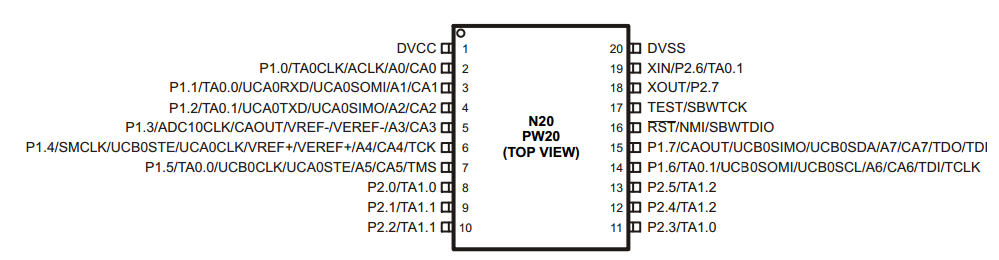
TI MSP430G2x53 Datasheet (SLAS735J )
These two pins must be configured to work with the USCI block by setting the applicable bits in P1SEL and P1SEL2 high. Recall the reason we put these pin configurations here and not in the driver is to help isolate the driver implementation from the board specific configuration. Now board_init should look like this:
[...]
    /* Configure P1.1 and P1.2 for UART (USCI_A0) */
    P1SEL |= 0x6;
    P1SEL2 |= 0x6;

    /* Configure P1.6 and P1.7 for I2C */
    P1SEL  |= BIT6 + BIT7;
    P1SEL2 |= BIT6 + BIT7;

    /* Global interrupt enable */
    __enable_interrupt();

    watchdog_enable();

    /* Initialize UART to 9600 baud */
    config.baud = 9600;

    if (uart_init(&config) != 0) {
        while (1);
    }

    if (i2c_init() != 0) {
        while (1);
    }
In a new header file include/i2c.h, we will define the I2C device structure which for now only consists of the device address of the slave device. In the future it may include other device specific parameters.
struct i2c_device
{
    uint8_t address;
};
Next we will write the transfer function. The transfer function should require the device structure as a parameter so that it can support multiple slave devices on the same bus. It should also be able to handle all three transaction formats so it will require two buffers, one to transmit and another to receive. It will also need to know the length of these buffers. Instead of making this function take a huge argument list, we will define another structure – i2c_data – in i2c.h which will encapsulate both transmit and receive buffers and their respective sizes.
struct i2c_data
{
    const void *tx_buf;
    size_t tx_len;
    void *rx_buf;
    size_t rx_len;
};
Now the transfer function only takes two parameters, the i2c_device structure and i2c_data structure.
int i2c_transfer(const struct i2c_device *dev, struct i2c_data *data)
{
    int err = 0;

    /* Set the slave device address */
    UCB0I2CSA = dev->address;

    /* Transmit data is there is any */
    if (data->tx_len > 0) {
        err = _transmit(dev, (const uint8_t *) data->tx_buf, data->tx_len);
    }

    /* Receive data is there is any */
    if ((err == 0) && (data->rx_len > 0)) {
        err = _receive(dev, (uint8_t *) data->rx_buf, data->rx_len);
    } else {
        /* No bytes to receive send the stop condition */
        UCB0CTL1 |= UCTXSTP;
    }

    return err;
}
The function begins by setting the slave device address in the UCB0I2CSA register. The following transactions will therefore be directed at this device. To support all three I2C transaction formats we need to first consider the transmit buffer. If there are bytes to transmit, these are sent first, so check the size of the transmit buffer is greater than zero – if so transmit the buffer. The actual writing of the buffer to the hardware is broken out into a separate function for the sake of keeping functions small and readable. Once the transmit is complete, and if there are no errors, then it’s time to see if the master needs to read any data from the slave. If so, then call the receive function. If there are no bytes to receive, then the transaction is complete and the master should issue the STOP condition by setting UCTXSTP in the UCB0CTL1 register.
Let’s quickly verify how this covers all three I2C transaction formats.
Master transmitter slave receiver: The transmit buffer will have data and therefore the length should be non-zero. Data will be transmitted to the slave. The receive buffer will have a length of zero so master does not receive any data from the slave. Therefore immediately after the transmit is complete the STOP condition will be set.
Master receiver slave transmitter: The transmit buffer will have a length of zero. Therefore the transmit section of the function will be skipped. The length of the receive buffer should be greater than zero and therefore the master will read that number of bytes from the slave and then the STOP condition will be set.
Combined format: In this case both the transmit and receive buffers are greater than zero. Start by transmitting the required number of bytes. If no errors have occurred, a repeated START condition will be issued and the master will receive data from the slave. Once that is complete, the STOP condition will be set.
Based on this quick analysis, we can see that this function will provide the flexibility required to support all three I2C formats and therefore should support any I2C slave device.
Now let’s take a look at how the driver transmits data from the master to the slave.
static int _transmit(const struct i2c_device *dev, const uint8_t *buf, size_t nbytes)
{
    int err = 0;
    IGNORE(dev);

    /* Send the start condition */
    UCB0CTL1 |= UCTR | UCTXSTT;

    /* Wait for the start condition to be sent and ready to transmit interrupt */
    while ((UCB0CTL1 & UCTXSTT) && ((IFG2 & UCB0TXIFG) == 0));

    /* Check for ACK */
    err = _check_ack(dev);

    /* If no error and bytes left to send, transmit the data */
    while ((err == 0) && (nbytes > 0)) {
        UCB0TXBUF = *buf;
        while ((IFG2 & UCB0TXIFG) == 0) {
            err = _check_ack(dev);
            if (err < 0) {
                break;
            }
        }

        buf++;
        nbytes--;
    }

    return err;
}
The transmission begins by setting the START condition. On the MSP430, this is done by setting UCTXSTT in the UCB0CTL1 register. Since the master is transmitting data to the slave, the UCTR bit needs to be set as well, which puts the USCI module in transmit mode. The hardware will now set the START condition and send the first byte with with I2C device address and R/W bit after which the UCTXSTT bit will be cleared and the transmit interrupt flag UCB0TXIFG in IFG2 set. Before transmitting the data however, we must check to make sure a slave acknowledged the initial byte. This is a common check, so it has been broken out into its own function which we’ll take a look at in more detail shortly. If the master received an ACK from the slave device, then it is safe to load the first data byte into the transmit buffer. Again we wait until the transmit interrupt flag is set and check for the ACK. The master must receive an ACK for every data byte before transmitting the next one. A slave device may NACK additional data if it busy so receiving a NACK would be an indicator to the master to stop transmitting. This cycle is repeated until all the data has been transmitted (or the transaction is forced to stop by a NACK). Notice at the end of the transmit function that we do not send a STOP condition because there may be data to receive, in which case a there should be a repeated START condition and not a STOP condition.
Next, let’s take a look at how the master receives data from the slave device.
static int _receive(const struct i2c_device *dev, uint8_t *buf, size_t nbytes)
{
    int err = 0;
    IGNORE(dev);

    /* Send the start and wait */
    UCB0CTL1 &= ~UCTR;
    UCB0CTL1 |= UCTXSTT;

    /* Wait for the start condition to be sent */
    while (UCB0CTL1 & UCTXSTT);

    /*
     * If there is only one byte to receive, then set the stop
     * bit as soon as start condition has been sent
     */
    if (nbytes == 1) {
        UCB0CTL1 |= UCTXSTP;
    }

    /* Check for ACK */
    err = _check_ack(dev);

    /* If no error and bytes left to receive, receive the data */
    while ((err == 0) && (nbytes > 0)) {
        /* Wait for the data */
        while ((IFG2 & UCB0RXIFG) == 0);

        *buf = UCB0RXBUF;
        buf++;
        nbytes--;

        /*
         * If there is only one byte left to receive
         * send the stop condition
         */
        if (nbytes == 1) {
            UCB0CTL1 |= UCTXSTP;
        }
    }

    return err;
}
Receiving data requires the master to send the START condition and slave device address byte but this time with the R/W bit cleared by clearing UCTR, putting the USCI module in receive mode. UCTXSTT is set to start the transaction and once the first byte is sent, UCTXSTT will be cleared by the hardware. Now the slave will begin sending data, but in the case of master receive mode the ACK is driven by the master rather than the slave. The master must NACK the last data byte it wants to receive. Otherwise, the slave does not know to stop sending data and a bus error or device error may result. If the receive buffer is only one byte, as soon as the first byte has finished transmitting, the stop bit, UCTXSTP in UCB0CTL1, must be set. In master receive mode setting this bit sends the NACK and then issues the STOP condition. The slave will still ACK the I2C device address byte, so this must be verified by the master. Assuming the ACK was received, the slave device will begin sending over data, each byte triggering the receive interrupt flag. Once the flag is set the data received is in the UCB0RXBUF register and can be read out. This is repeated for all data bytes until there is only one left to receive. The master must NACK the last data byte and then issue a STOP condition, so before receiving it we must set UCTXSTP.
Finally, let’s take a look at how to handle the N/ACK from the slave device.
static int _check_ack(const struct i2c_device *dev)
{
    int err = 0;
    IGNORE(dev);

    /* Check for ACK */
    if (UCB0STAT & UCNACKIFG) {
        /* Stop the I2C transmission */
        UCB0CTL1 |= UCTXSTP;

        /* Clear the interrupt flag */
        UCB0STAT &= ~UCNACKIFG;

        /* Set the error code */
        err = -1;
    }

    return err;
}
There are a few conditions in which the master might receive a NACK as we have seen. It could be the address does not match, or the slave can no longer receive any data. To check for a NACK, the NACK interrupt flag field, UCNACKIFG in the status register UCB0STAT, should be read. When the master receives a NACK, it should abort the transaction. Therefore, it must send a STOP condition and should clear the interrupt flag.
Using the driver to write and read data
Now that the driver is written, we can use it to store data to the EEPROM. Lets connect the breadboard to the MSP430 LaunchPad. Vcc and ground are straightforward – they are simply connected to the Vcc and ground pins on the LaunchPad. Pins P1.6 and P1.7 were configured for SCL and SDA respectively in board.c, so those pins can be connected to the EEPROM pins 6 and 5 on the breadboard.
To test out our driver, we will create two new menu options to read and write a single byte to the EEPROM. Currently they only support reading and writing one byte of data but they could be extended to ask the user for a length, or you can modify the code to change the size of the buffers.
static int eeprom_read(void)
{
    int err;
    struct i2c_device dev;
    struct i2c_data data;
    uint8_t rx_data[1];
    uint8_t address;

    dev.address = 0x50;

    address = (uint8_t) menu_read_uint("Enter the address to read: ");

    data.tx_buf = &address;
    data.tx_len = sizeof(address);
    data.rx_len = ARRAY_SIZE(rx_data);
    data.rx_buf = (uint8_t *) rx_data;

    err = i2c_transfer(&dev, &data);

    if (err == 0) {
        uart_puts("\nData: ");
        uart_puts(_int_to_ascii(rx_data[0]));
        uart_putchar('\n');
    }

    return err;
}

static int eeprom_write(void)
{
    int err;
    struct i2c_device dev;
    struct i2c_data data;
    uint8_t write_cmd[2];

    dev.address = 0x50;

    write_cmd[0] = menu_read_uint("Enter the address to write: ");
    write_cmd[1] = menu_read_uint("Enter the data to write: ");

    data.tx_buf = write_cmd;
    data.tx_len = ARRAY_SIZE(write_cmd);
    data.rx_len = 0;

    err = i2c_transfer(&dev, &data);

    return err;
}
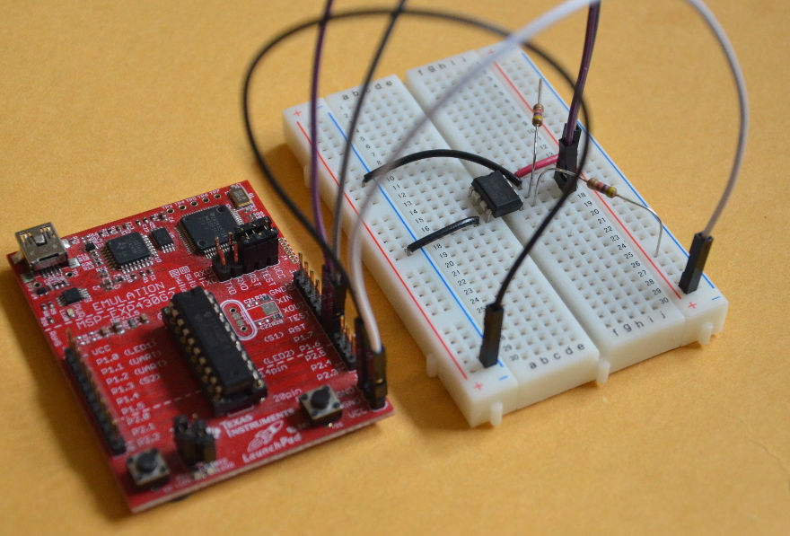
In both cases the user is asked to enter the address. The read function points the transmit buffer to the address and sets the length to 1 byte, which is standard for this device (other EEPROMs or I2C devices that have a bigger address space may require more than 1 byte for the address). The receive buffer points to the rx_data array, which has been defined with one element. If you want to increase the number of bytes read, the size of this array can be modified. The i2c_transfer function is called and and the received data is printed out to the serial port. For example, try to read the data at address 0x7 – here is a screenshot of the I2C transaction from an oscilloscope.
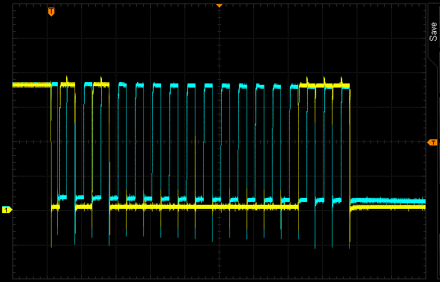
The blue trace is SCL and the yellow trace SDA. We can see the first byte being transmitted is 0xA1 ((device address << 1) | write = (0x50 << 1) | 0x1 = 0xA1). On the 9th clock cycle, the SDA line is low, indicating that the EEPROM acknowledged the first byte. Then the address to read from is transmitted. Over the next 8 clock cycles, the SDA line toggles to 0b00000111 = 0x7. Again on the 9th clock cycle the EEPROM acknowledges. Since a read is a combined format transaction, both SDA and SCL are released high and the repeated START condition is issued. However, at the end of the first image, you can see both lines are held low for quite some time. This is called clock stretching and it is implemented by the hardware to delay the next byte in the transaction. In this case, the EEPROM is saying ‘wait for me to retrieve the data!’. When it is done, the master can continue clocking in the byte. Now the first byte is 0xA0 ((device address) << 1 | read = (0x50 << 1) | 0 = 0xA0). The EEPROM acknowledges once more and the next 8 clock cycles it transmits the data byte back to the master. In this case the data at address 0x7 was 0xFF – the ‘erased’ value of an EEPROM. The transaction ends with the STOP condition and both lines return to idle.
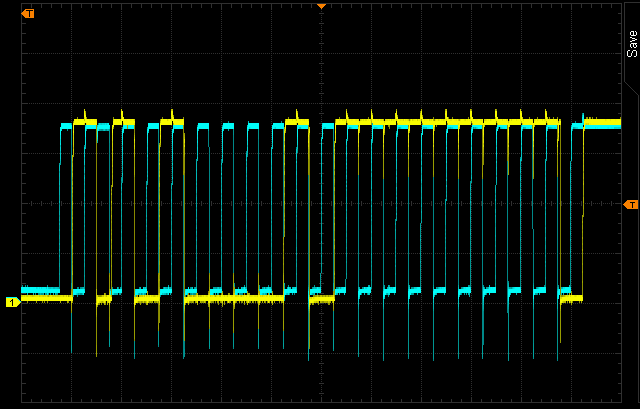
The write function is similar except that the user is also prompted for the value to write. The transmit buffer is pointed to the write_cmd array which has a length of 2 bytes, one for the address and the other for the data. Again, this could be increased in size to write more data. The receive buffer isn’t set but the length must be set to 0 to indicate to the driver there are no bytes to receive. If I now write the value 55 (0x37) to address 0x7, the transaction will look like this:
The first byte being transmitted is 0xA1 ((device address << 1) | write = (0x50 << 1) | 0x1 = 0xA1). On the 9th clock cycle, the SDA line is low, indicating that the EEPROM acknowledged the first byte. Then the address to write is transmitted. Over the next 8 clock cycles, the SDA line toggles to 0b00000111 = 0x7. Again on the 9th clock cycle the EEPROM acknowledges and then the master starts to transmit the data and we can see the SDA line toggle to 0b00110111 = 55. The transaction once again ends with the STOP condition and both lines return to idle.
This test code is not really how an EEPROM would be accessed in practice but at least we can test our interface, driver and hardware setup. In the next tutorial we will look more at reading and writing from the EEPROM and demonstrate some real-life use cases.